As the demand for high-performance materials increases, so does the importance of surface engineering. The material’s surface is its point of interaction with the external environment and other materials, and will influence factors such as corrosion rates, catalytic activity, adhesive properties, wettability, contact potential, and failure mechanisms.
Surface modification can be used to alter or improve these characteristics; surface analysis is used to understand surface chemistry and investigate the efficacy of surface engineering. From non-stick cookware coatings to thin-film electronics and bio-active surfaces, X-ray photoelectron spectroscopy is one of the standard tools for surface characterization.
X-ray photoelectron spectroscopy (XPS), also known as electron spectroscopy for chemical analysis (ESCA), is a technique for analyzing a material’s surface chemistry. XPS can measure elemental composition as well as the chemical and electronic state of the atoms within a material.
XPS spectra are obtained by irradiating a solid surface with a beam of X-rays and measuring the kinetic energy of electrons that are emitted from the top 1-10 nm of the material. A photoelectron spectrum is recorded by counting ejected electrons over a range of kinetic energies. The energies and intensities of the photoelectron peaks enable identification and quantification of all surface elements (except hydrogen).
Surface characterization
The surface represents a discontinuity between one phase and another; the physical and chemical properties of the surface are, therefore, different from those of the bulk material. These differences affect the topmost atomic layer of the material to a large extent because a surface atom is not surrounded by atoms on all sides. This results in the surface atom having a bonding potential, which makes it more reactive than atoms in the bulk.
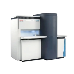
XPS X-Ray Photoelectron Spectroscopy
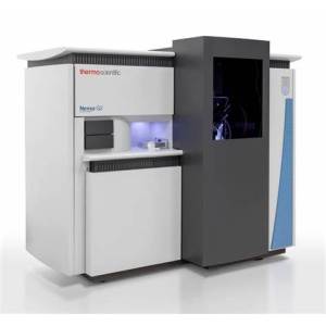
XPS X-Ray Photoelectron Spectroscopy
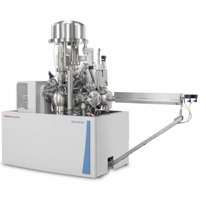
XPS X-Ray Photoelectron Spectroscopy