FIB-SEM is a technique that combines the high-resolution imaging of a scanning electron microscope (SEM) with the precise sample modification of a focused ion beam (FIB). FIB-SEM can be used for a variety of applications, such as:
– Site-specific analysis, deposition, and ablation of materials, especially in the semiconductor industry and materials science1.
– Preparation of high-quality and thin samples for transmission electron microscopy (TEM) from a wide range of materials2.
– Subsurface and 3D characterization of structures by sequential FIB milling and SEM imaging2.
– Nano-prototyping and patterning of devices by FIB etching and deposition2.
FIB-SEM is a powerful and versatile tool that can reveal nanoscale information and enable novel experiments for many scientific and engineering fields.
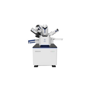
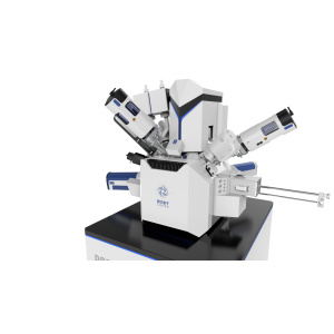
FIB-SEM Dual Beam Microscopy